

What is PWM ?
Pulse Width Modulation (PWM) is a 'digital' way to drive DC 'servo' motors that will conserve battery power. Instead of amplifying the 'drive demand' voltage, a digital 'chopper' circuit turns the 'demand' voltage into a stream of 'on/off' pulses with a variable width 'on' (or 'mark') to 'off' ('space') ratio
During the 'mark' time the full supply voltage is applied to the motor. During the 'space' time, no voltage is applied. Because the stream of 'mark/space' pulses are applied at high speed, the motor can only respond to the average voltage applied. So, for example, when the mark / space ratio is 50:50, the motor 'sees' half the supply voltage (and runs at half speed).
So long as the 'on' and 'off' switching transitions are 'fast', almost no power is consumed in the (transistor) switching circuit. At 'half speed' (50/50 mark/space) the drive will be taking 50% power from the supply and delivering it all to the motor (unlike a variable voltage control circuit amplifier, where 100% power is always taken from the supply, and, at half speed, half the power is applied to the motor whilst the other half is dissipated as heat in the amplifier).
RC ('Radio Control' - for model aircraft) 'servo motors'
These are special case geared motors with built-in PWM drive circuits to control the 'position' (rather than the speed) of the shaft. These motors are 3-wire (power and Gnd for the drive circuits, 1 wire 'pwm' control). The 'pwm' control signal has a fixed frequency (typically 30-50Hz**, may be lower). The duty cycle (from about 10%-90%) determines the shaft position. Positional feedback is typically via an attached (or built-in) potentiometer.
** the response speed of the 'classic' or 'analogue' RC servo motor is limited by the pwm control (50Hz = 20mS). To improve response speeds, newer RC motors have circuits that will accept pwm control frequencies from 300Hz up to 400Hz (these are typically known as 'digital RC servos', both to differentiate them from the older 50Hz type and, no doubt, to justify the rip-off pricing)
What are the drawbacks of PWM ?
A1. A simple circuit is typically unable to control the motor all the way from 'stopped' (0 mark, 100% space) to 'full power' (100% mark, 0% space). Fortunately, for star tracking, we only need to vary the motor speed slightly about some 'nominal' speed.
One way to achieve 'full rated speed' using a PWM circuit that starts at 'zero' but 'tops out' at (say) 90% mark is to use an over-voltage supply - at 90% mark/space a 110% supply would deliver ('on average') 99% of the rated voltage to the motor.
A2. To avoid the possibility of any audible 'whine', the frequency of the mark/space pulses must be over 20kHz.
In motorised telescope star tracking mount drives, we will almost always have available a quartz crystal controlled 'time clock' reference. This typically uses the 32.768 kHz quartz crystal controlled oscillator chip known as the CD4060. This is a 14-stage divider (so final o/p is 2 Hz), however pin (9) is a buffered o/p of the 32.768 kHz oscillator. This signal (32khz) can be fed straight to the PWM control circuit (and maybe used to drive a PIC controller, however that's another story).
Designing a PWM drive circuit
Given an existing clock source, a basic PWM consists of 2 basic stages ...
1) The generation of the 'demand' or 'control' voltage (Vctl), proportional to the required motor speed (i.e. the signal that would normally be amplified and used to directly drive the motor in a analogue servo drive design).
In theory the Vctl control signal varies from 0v to Vmax in a linear fashion, such that 0 = motor stop, Vmax/2 = motor half speed, Vmax = motor full speed. In practice, the signal 'range' will be limited to vary about some 'nominal' motor speed (e.g. +/- 10% from 90% speed).
2) Conversion from the 'demand' voltage (Vctl) into a 'mark-space' pulse train.
Typically this involves some sort of comparison between the 'demand' voltage and a saw-tooth (or 'ramp') reference generated by the pulse clock.
A pulse starts 'on' ('mark') and stays 'on' until the ramp voltage exceeds the demand voltage at which point the 'mark' is switched 'off'. The pulse then remains 'off' (in 'space') until the next clock triggers 'on' again.
It is difficult for such a system to achieve 100% 'mark' simply because there must always be some 'space' time, at the end of the current 'mark', so the ramp generation circuit (usually a capacitor/resistor driven from the clock pulse train) can be reset (discharged) and the ramp returned to 'zero' before the next clock 'trigger' arrives.
Instead of a 'ramp' (saw tooth) the clock could be used to generate a triangle wave. If the clock is a 'reasonable' square wave this can be achieved directly by clock = Hi 'ramp up' and clock = Lo 'ramp down'. If 'down' rate*time is 'harder' then the 'up' rate*time the 'triangle' will always return to zero. In this configuration, the 'demand' voltage can be used to control the 'space' time (i.e. when the ramp exceeds the demand, 'space' is output) and 100% 'mark' can now be achieved (when demand is higher than the maximum possible ramp).
The problem with this approach is that adjusting the demand max to 'max ramp' (apex of the triangle) becomes a critical setting (since '1 voltage step lower than max' must be 'some space'), HOWEVER if 99.9% (as opposed to 100%) of maximum speed is acceptable (as it should be in practice) it should be easy to set-up so that demand 'max' just 'clips' the top of the triangle.
As is always the case with analogue electronics, considerable care must be taken to avoid control signals 'drifting' in different directions when the voltage or temperature varies.
One other thing to watch out for is that the apex of the triangle does not occur at the same time as the clock is triggering the 'speed count' circuit.
Do you have a 'real world' circuit ?
Browsing the web you will find many circuit diagrams being offered that claim to 'solve' your PWM problems. Needless to say, they are full of "Rn's" and "Cx's" (with comments such as 'choose R & C as appropriate', sometimes with some theoretical 'formula' like "set t=1.1RC"). Often the supply voltage is simply left out altogether (despite the fact that the performance any analogue IC (such as the NE555 timer) is totally dependant on the supply meeting some minimal voltage spec).
Of course almost none of these circuits have ever actually been constructed (in fact, you can guarantee than no circuit with an 'x' in it (Rx, Cx etc) will have been built 'for real).
The only way to determine if any particular circuit will work at all is to generate a SPICE simulation - at which point you will discover the vast majority of 'web' PWM circuits are incapable of actually working at all, no matter what values of R 'x' & C 'x' you set.
For this reason it's a very good idea to first simulate your circuit (e.g. using LT SPICE) and then 'breadboard' it before getting out the soldering iron :-)
Things that simulation will reveal :-
Many analogue circuits can be so dependant on the supply voltage that it goes from non-working, to working (more or less) 'as intended' and then into a 'locked up' or 'part working' mode as you change the supply by just a volt or two (so once you have it working, change your supply voltage and see what happens - or give up on using a battery supply for ever :-) )
Adding even a tiny capacitive 'loading' (e.g. the base of a transistor) to parts of a circuit involved with timing can have a massive effect on waveform shapes and frequencies - and again turn working circuits into a non-working ones (or, indeed, vice-versa). When you have to start using 1nF capacitors or 1m (1,000k) resistors to get the circuit to work at all, you need to start worrying :-)
You will discover that the 'SPICE' (simulation) 'models' of anything except basic resistors, capacitors and inductors (and ESPECIALLY IC's such as 555 timers) are 'approximate' at best .. different models of the 'same' device (e.g. standard NE555 V's' low power' TLC555) can behave completely differently, especially in terms of current source/drains. Sometimes a model may even be missing parts of the basic functionality !
One 'feature' of the simulation software allows 'back propagation' of loading effects from outputs into inputs - this can have totally unexpected effects on remote parts of the circuit resulting in completely unexpected (and hard to track down) behaviour. You will be surprised to discover 'low power' transistor models that appear to sink multiple-tens of Amps at their 'base' and both transistors and IC's apparently delivering voltage swings of 800v or more at their outputs, especially when inductive loads exist elsewhere in the circuit.
Active components do not perform in 'ideal' ways - specifically, IC outputs and transistor transition times (due to real world capacitive loadings) will turn your perfect 'square wave' drive at the input (or base) into a 'rounded corner' sine wave (or ramp / triangle wave) at the output (collector / emitter), especially when you attempt to achieve (near) rail-to-rail voltage swings.
When designing circuits using low voltage supplies (e.g. 6v battery), voltage drops across diodes and transistors are very significant (so, for example, it is not possible in practice to drive a 6v motor form a 6v battery (unless you use a relay at the final power stage) .. even driving it from a 7.2v (rechargeable stack) may prove extremely difficult).
Almost all digital logic circuits are better at driving 'Lo' (o/p voltage near ground) than they are at sourcing Hi (o/p voltage near supply).
Using the NE555 timer chip
The standard 555 timer is capable of sourcing or sinking 200mA at it's output pin3 (and sinking 200mA at the 'discharge' pin7) and contains a voltage comparator (threshold V control pin6).
When 'trigger' (p2) is lower than the internal reference, the latch is 'set' and the output goes 'Hi' and discharge p7 is 'off' (high impedance).
When 'threshold' (p6) goes above 'control' p5 the latch is 'reset' and output goes 'Lo' and discharge p7 is turned 'on' (sink). 'Reset' Lo also forces the latch into 'reset'.
If trigger p2 is Lo whilst threshold p6 is Hi, the IC can oscillate (although apparently the p4 reset overrides the trigger)
In below:-
The 32 kHz signal (V1) is buffered via a diode (D1) to a capacitor (C2) that is wired via a 1k resistor (R17) to +V (7.2v). When the 32kHz 'square wave' goes Lo, the cap C2 is discharged quickly & held Lo. When the 32 kHz goes hi, the cap charges up slowly via the resistor. We thus have a 'ramp' which we can apply to the 'threshold' p6 where it is compared to the control (demand) voltage on p5. The demand voltage will always be higher than half the supply voltage (7.2v) level ... so the 32 kHz ramp can be applied to the trigger (p2) where (when it is Lo) it will 'set' the latch.
The latch remains set until the ramp exceeds the control .. thus the 'on' time is determined by the voltage from the R-2R ladder D-A converter (the latch stays on until reset as ramp climbs above control).
SPICE Circuit diagram
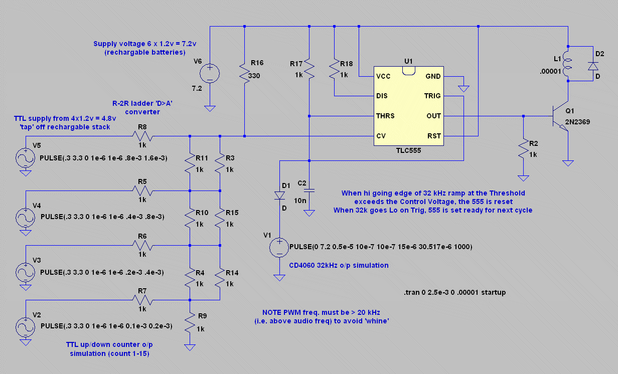
Note that in above the NE555 has been 'mirror imaged' to make the SIMULATION layout easier to understand (pin 1 is GND, pin 8 VCC). To avoid confusion, you will need to draw a WIRING DIAGRAM (with the chip in it's correct orientation) before constructing the actual circuit.
Note also the final output drive is buffered by the 2N2369 power transistor (L1, 1uH represents the motor, D2 is the 'fly wheel' diode that protects the transistor from 'back emf' (D1 needs to be 'high power' (1A should do) as the transient current (from the inductive motor coil) can be quite high)
Finally, note that whilst the NE555 chip may be able to source/sink 200mA and this may allow you to drive the motor directly, you will end up replacing a lot of NE555's whilst experimenting (especially if you forget the 'back emf' diode or accidentally 'short out' the drive) etc.
SPICE simulation results
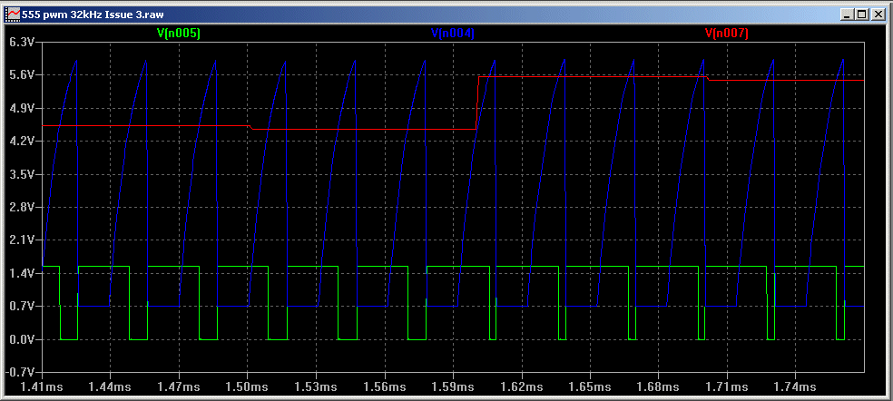
In the trace above, Red = 'demand' voltage (U1 CV), Blue = ramp (U1 THRS & TRIG), Green = U1 OUT (drive to base of Q1 transistor).
The trace shows (Red) count down from 1 to 0 & then from 15 to 14 & the (Green) corresponding change in the output mark/space ratio from minimum to max.
The 'minimum' speed = count 0 = mark/space approx 70% delivering approx 5v 'average' to the 6v motor. The 'maximum' = count 15 = mark/space approx 91% delivering 6.5v to the motor. The voltage varies by 1.5v as the count varies from 0 to 15. With each count 'worth' approx .1v, the motor will see it's rated voltage (6v) at count = 10, which is not too far off the 'ideal' mid-position (count 7 or 8)