

PIC16F5xx based Video Time Inserter (VTI)
The biggest problem with using the 16F5x is detecting the Frame Sync and Line Sync from the incoming AV signal. What's needed is a PIC with an analogue comparator capability, such as the PIC16F526 (available for less than £1), although the 16F5xx has the same instruction set and max. frequency specification as the 16F5x, so is still limited to 'chunky' (double width) characters (unless an 'external' shift register is used, see below).
For a single-chip 'skinny' character display, you need a PIC that can deliver pixels at about 12MHz, which means a 12MHz CPU (i.e. 48MHz OSC) - and that means using one of the 18Fxxx devices (see my PIC18F VTI page).
A common requirement for any CCTV system is to insert the date and time in a 'guaranteed' way that avoids any possibility of error. Essentially, this means adding the date/time to the 'live' AV video feed (i.e. before it is recorded) using a GPS or NTP source derived date and time. This means building a type of On Screen Display (OSD) device known as a Video Time Inserter (VTI)
Basic CCTV systems use the NTSC standard, either 'half frame' (240 lines) or 'interleaved' (480 lines) at 60Hz. The half frame pixel count is 320, for interleaved, it's 640. The 'full' PAL video is 625 lines (312.5 interleaved) at 50 Hz (of which 576 lines are 'visible', with 768 'square' pixels per line).
To discover what standard is in use, the VTI can detect the 'frame Sync' and then count the number of lines in a frame. It's usual to use a LED to indicate when frame sync / line sync has been 'detected' (to provide feedback for manual adjustment)

From the line count, the PIC can 'work out' where to start inserting the date and time (usually 10 lines from the bottom of the frame - although if 'spare' pins exist, it's easy enough to provide a manual means of changing the insert position)

The AV pixel rate is irrelevant - the PIC will be outputting pixels at it's maximium possible rate at all times, however it would be 'an advantage' to provide a measns of manually adjusting the insert start position (from the left)
The PIC16F526
With the same rated speed (20 MHz OSC) and instruction set as the 16F5x, this 14pin device has 1k instruction space, 67 GP registers, 68 bytes of flash memory, an 8 bit A-D converter and two analogue comparators. One comparator has a fixed '0.6v' reference and the other a programmable on-chip Reference voltage
The i/o pins are arranged into 2 groups, PORT B and C, each of 6 bits. To output a 5 pixel wide font, 4 LSB pins - bit0 to bit3 - are required.

Bit 3 on PORT B is the Master Clear, which we need as an input (so we can reset a locked up chip), so can't be used for 'pixels out'

This means PORT C is the 'pixel shift register', however the PORT C comparator is the one with the programmable Vref. This means we have to use the PORT B comparator (with the fixed 0.5-0.7v (0.6v nominal) Vref) to detect Hsync and Vsync (more later)

RB0 Compare1 in V+ / InCircuit Prog (ICSP) Data
RB1 [spare] (comp1 in V-  / InCircuit Prog (ICSP) Clk
RB2 Compare1 Out
RB3 MClr in (master clear)
RB4 CPU Clk out (OSC/4) when using EC mode)
RB5 EC mode CLOCK (OSC) in
Video Sync detect (comparator operation)
The comparator input(s) are protected with diodes to Gnd and Power V+, so (assuming 5v Power) the input must be within -0.6v and +5.6v. When the internal 0.6v (nominal) Vref is used, the output will be '1' when the V+ input is above 0.6v (and 0 when below 0.6v) i.e Sync = 0.
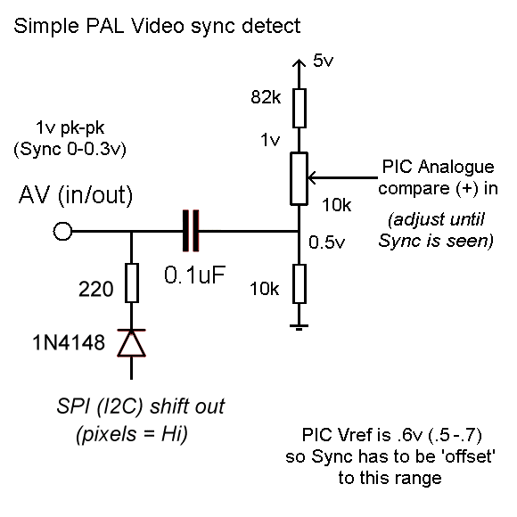
The incoming Video signal is (nominally) 1v peak-to-peak, with '100%' (Hi) = white pixels, '33%' = 'black' and '0%' (Lo) = Sync.
If the Video signal source drive is 'AC coupled' (using a capacitor), you can expect the '1v peak to peak' to be +0.5v to -0.5v. However, often it is 'DC coupled' and you will see 0v to +1.0v, which puts Sync at 0-0.3v (and 'white pixels' at 1v).
Fortunately, it's quite easy to 'buffer' the incoming Video with your own capacitor and apply your own 'DC offset' (to shift the Sync voltage up or down on your side of the capacitor) to get a +0.6v Sync level from both AC coupled +/-0.5 or DC 0-1.0v
One thing to watch out for is the 'colour burst'. Most CCTV (and web-cams) cameras will generate a colour Video stream and this means they will insert a 'colour burst' signal between each HSync pulse and the start of the line of (B&W) pixels. The 'colour burst' signal is approx +/- 0.15v from (i.e. above and below) the black (0v) level. This means to 'guarantee' detection of HSync (rather than part of the colour burst) you have to trigger only when the input AV is from 0.2v to 0.3v below the black ("0v") level
On a DC coupled 0-1v Video signal, you should look for Sync from 0-0.1v, on 'true' AV signal, it's -0.2 to -0.3v.

To use the PIC comparator, the Sync has to be 'moved' to the voltage expecrted by the PIC, i.e. .6v +/-.1 V. To do this, you have to AC couple the Video input to a resistor 'ladder'. The PIC comparator is expecting 0.6 v, so the resistor ladder has to 'shift' the incoming 0-1.0v range to 0.5-1.5v.

The PIC internal 'fixed' Vref is only 'nominally' 0.6v = it can be anything from 0.5-0.7v. So you have no choice but to use a variable resistor to 'tap off' the shifted Video to the PIC comparator input.

Note that you can 'get away with' driving the raw Video input (i.e. both DC 0-1v and AC +/-0.5v) to 1.0v when inserting 'white' pixels. This lets you wire the PIC 'output pixel' pin 'direct' (actually, via a diode, so you get white pixels over the background video rather than white pixels on a black background) to the AV input
Sync detect Timing
The comparator output typically takes 150nS (400nS max) to respond when it's input crosses the Vref threshold (which with a 25MHz/40nS OSC i.e. 160nS CPU CLK, this is about 1-3 CPU CLK cycles).
To 'spot' the Sync, it's tempting to use the PIC 'wake up on compare' (change) function. On wake up, the PIC performs a RESET (jump to 0) with status bits set to indicate the 'cause' of the Reset (Power-on, WDT, TMR0, pin state change etc).

If an external Osc is used, Wake Up time (DRT) will be "10uS". At 25MHz / 40nS per cycle OSC, 10uS is 250 OSC cycles or 62.5 CPU cycles ... which means our timing can 'slip' by 0.5 CPU cycles each time we 'wake up' = not good ... however at a guess, the '10uS' is an 'analogue' delay, so won't be 'exact' anyway (so the 'slip' is likely multiple CLK cycles)

If we use a simple program 'loop' (test the comparator bit and skip, else jump back), the 'detect' is a 'guaranteed' 1-2 CPU clock ctycles. However if we use this to decide the start of a scan line, the position of successive lines of pixels could differ by 1-2 CPU CLKs's !

To 'stabilise' the output of pixels, the PIC 'shift out' must be 'locked' to Video HSync. One way to do this is to ASSUME the Video source is stable and 'trigger' only once per frame. This 'works' so long as there is an exact (integer) number of PIC CPU clock cycles 'per Video scan line'.
Avoiding 'tearing' and 'jitter'
Sync detect gets us from the 'top of the frame' (VSync) to the first 'insert position' scan line (N x HSync). At this point, we can assume the Video generation is stable enough to simply 'count' complete lines (at 64uS intervals) for the entire VTI process, rather than continue to look for HSync and 'get it wrong'
Whilst this 'guarantees' the insertion of pixels for all 7 scan lines of the character will be 'stable' (i.e. no 'tearing'), 'jitter' is still possible due to variable frame sync detect timing
Jitter is due to an 'early' or 'late' detect of HSync on the next frame that 'shifts' the whole insert process by one CPU CLK (i.e. 1 pixel)
The problem is two fold. First both the Video generation OSC circuit and PIC OSC can 'drift' very slightly due to temperature etc. Whilst this drift may not be significant over 448uS (7 scan lines), over a complete (half) frame of 20mS it's another matter.

Second, whilst the Video frame rate may be an integer number of CPU CLK's (so, in theory, we should always 'see' the Sync's on the 'same' CLK) the Sync may happen to fall on (or very close to) a CPU CLK boundary.

In that case, even a very slight OSC change - or tiny change in the 'Sync detect' (such as Vref variation due Power V+ glitches etc.) - would be enough to 'push' the Sync detect from one CPU CLK to another (which moves the entire VTI by a whole pixel)
To 'fix' to the jitter problem we either have to 're-sync' the PIC CPU CLK or 're-sync' the pixels
If Sync detect can be performed at PIC OSC intervals, the detect accuracy goes from 1 pixel (1 CPU CLK) to 1/4 pixel (1 OSC cycle).

This need not be as hard as it seems - the 'raw' Comparator output is alreaedy available on pin RB2, and the CPU CLK on TB4 - so 'all' we need to do is 'delay' the PIC OSC by 1,2 or 3 cycles if the 'detect' happens to fall on the 'wrong' part of the CPU OEC cycle.
The alternative to 'moving' the CPU CLK is to 'move' the output pixel. The PIC output pin can be wired to an external circuit (shift register) clocked at OSC frequency from a circuit that is 'restarted' on every Sync detect (the idea being to delay the pixel by 1-4 OSC cycles (or 0-3)).

The port pin changes state at the end of Q4, i.e. on the trailing edge of the CPU CLK (which is the leading edge of the Q1 OSC).
Pixel output (PIC shifting)
At best, we can output pixels at CPU CLK rate (using ROTL on one of the PORTs).
To output a 5 bit character shape wide Font, we need to dedicate all 4 of the 'low' bits (b3-b0) of a PORT (the 5th bit is supported by loading the shape to the Acc using a ROTR instruction, so the shape b0 starts in Cy, whilst shape bit 4 is output on the PORT b3)).

The ROTL PORT will read the whole PORT, shift the 6 bits 'up' and save the rotated result to the output latch. This means the upper 2 bits of the PORT can be used as inputs (but not outputs), so long as 'reading' those inputs has no adverse effect.

The  inter-character 'gap' zero bits can be 'output' using CLR PORTC.

Since loading the next shape requires 1 CPU CLK, during which the current output bit won't change, we can only 'load' after 'setting up' the first 'zero' of a  2 zero inter-character gap

The output format is 'DD mm 20YY    hh:mm:ss.ss'

Each pair of characters is separated by an inter-character gap of 2 zeros. The DD mm (and mm 20YY) gap is 5 zeros. The date / time gap is at least 10 zeros. The ' and : consists of 2 zero gap, 1 bit mark, 2 zero gap.

The 'easy' way to deal with the . and : is to add them to the character shape any only 'shift them out' if needed. This requires one extr bit from the PORT (we can use BitClr on the PORT pin for the gap and then rotate for the final bit)

DD) Output starts with the '10 of Day' number, 5 bits wide, followed by 2 'zero' bits, then Day units, 5 bits followed by 6 'zero' bits of gap.
mm) same as DD
20) Fixed '2' 5 bits, 2 gap then fixed '0' 5 bits, 2 gap
YY) same as DD
) gap - at least 10 bits
hh :) 10 of hours 5 bits, gap 2 bits, unit hours 5 bits, gap 2 bits, fixed ':' 1 bit, gap 2 bits
mm :) same as hh :
ss.ss) 10 os seconds 5 bits, 2 gap, units seconds, 2 gap, fixed '.', 2 gap, 1/10ths of second, 2 gap, 100/ths seconds.

To avoid 'wasting' extra registers on the ':' and '.' these will be incorporated into all the shapes as bit0.  The 5 bits of the actual shape will thus be in b1-b5. All shapes will be ROTR'd (so b0 goes into Cy) before output starts. PORTC C, b4 is the Video out (PORT C bit5 is spare).

To output the first bit, we COPY Acc to PORT C. After 4 ROTL we BCLR PORTC b4 (to output the first gap zero). If this is to be followed by the '.' or ':' we perform a single NOP, then another ROTL before another BCLR PORTC b4. Whilst the second gap zero is output, we load the next Register to Acc with a ROTR.

There is no time to perform JUMP or CALL within the Video out sequence, so the entire output code has to be 'in-line'
VideoOut:
; Video output subroutine, called 8 times to output 5x8 shapes (uses second stack for delay)
; Character shape (5) + punctuation is in Register bits 0 to 5
; bit5 = MSB = first (left most) bit of the 5 shape bits
; ROTR is used to move b0 into Cy (where it will be the last bit o/p) and thus MSB b5 into Acc b4
; PORT C bit4 is the Video out
;
ROTR RegD10, Acc	;get 10's of days (b0 to Cy)
COPY Acc,PORTC		;shape b5 (Acc b4) to o/p
ROTL PORTC			;shape b4
ROTL PORTC			;shape b3
ROTL PORTC			;shape b2
ROTL PORTC			;shape b1
CLR PORTC			;gap 1
ROTR RegD1, Acc		;get 1's of days (b0 to Cy) whilst output gap2
COPY Acc,PORTC		;shape b5 (Acc b4) to o/p
ROTL PORTC			;shape b4
ROTL PORTC			;shape b3
ROTL PORTC			;shape b2
ROTL PORTC			;shape b1
CLR PORTC			;gap 1
CALL aReturn		;4 CPU CLK's, output 4 gap zero's
ROTR Regm10, Acc	;get 10's of month (b0 to Cy) whilst output gap6
COPY Acc,PORTC		;shape b5 (Acc b4) to o/p
ROTL PORTC			;shape b4
ROTL PORTC			;shape b3
ROTL PORTC			;shape b2
ROTL PORTC			;shape b1
CLR PORTC			;gap 1
ROTR Regm1, Acc		;get 1's of month (b0 to Cy) whilst output gap2
COPY Acc,PORTC		;shape b5 (Acc b4) to o/p
ROTL PORTC			;shape b4
ROTL PORTC			;shape b3
ROTL PORTC			;shape b2
ROTL PORTC			;shape b1
CLR PORTC			;gap 1
CALL aReturn		;4 CPU CLK's, output 4 gap zero's
; (30 instructions so far)
; Next up is the 'fixed' shape 20, however this will still have to be held in registers (there is not enough time to look up the shapes)
ROTR RegY2, Acc		;get '2' year (b0 to Cy) whilst output gap6
COPY Acc,PORTC		;shape b5 (Acc b4) to o/p
ROTL PORTC			;shape b4
ROTL PORTC			;shape b3
ROTL PORTC			;shape b2
ROTL PORTC			;shape b1
CLR PORTC			;gap 1
ROTR RegY0, Acc		;get '0' year (b0 to Cy) whilst output gap2
COPY Acc,PORTC		;shape b5 (Acc b4) to o/p
ROTL PORTC			;shape b4
ROTL PORTC			;shape b3
ROTL PORTC			;shape b2
ROTL PORTC			;shape b1
CLR PORTC			;gap 1
ROTR RegY10, Acc		;get 10's of Year (b0 to Cy) whilst output gap6
COPY Acc,PORTC		;shape b5 (Acc b4) to o/p
ROTL PORTC			;shape b4
ROTL PORTC			;shape b3
ROTL PORTC			;shape b2
ROTL PORTC			;shape b1
CLR PORTC			;gap 1
ROTR RegY1, Acc		;get 1's of year (b0 to Cy) whilst output gap2
COPY Acc,PORTC		;shape b5 (Acc b4) to o/p
ROTL PORTC			;shape b4
ROTL PORTC			;shape b3
ROTL PORTC			;shape b2
ROTL PORTC			;shape b1
CLR PORTC			;gap 1
CALL aReturn		;4 CPU CLK's, output 4 gap zero's
CALL aReturn		;4 CPU CLK's, output 4 gap zero's
; now the hh:mm:ss.ss set (60 so far)
ROTR RegH10, Acc	;get 10's of hours (b0 to Cy)
COPY Acc,PORTC		;shape b5 (Acc b4) to o/p
ROTL PORTC			;shape b4
ROTL PORTC			;shape b3
ROTL PORTC			;shape b2
ROTL PORTC			;shape b1
CLR PORTC			;gap 1
ROTR RegH1, Acc		;get 1's of hours (b0 to Cy) whilst output gap2
COPY Acc,PORTC		;shape b5 (Acc b4) to o/p
ROTL PORTC			;shape b4
ROTL PORTC			;shape b3
ROTL PORTC			;shape b2
ROTL PORTC			;shape b1
CLR PORTC			;gap 1
NOP					;gap 2
ROTL PORTC			;shape b0 : out
CLR PORTC			;gap 1
ROTR RegM10, Acc	;get 10's of mins (b0 to Cy)
COPY Acc,PORTC		;shape b5 (Acc b4) to o/p
ROTL PORTC			;shape b4
ROTL PORTC			;shape b3
ROTL PORTC			;shape b2
ROTL PORTC			;shape b1
CLR PORTC			;gap 1
ROTR RegM1, Acc		;get 1's of mins (b0 to Cy) whilst output gap2
COPY Acc,PORTC		;shape b5 (Acc b4) to o/p
ROTL PORTC			;shape b4
ROTL PORTC			;shape b3
ROTL PORTC			;shape b2
ROTL PORTC			;shape b1
CLR PORTC			;gap 1
NOP					;gap 2
ROTL PORTC			;shape b0 : out
CLR PORTC			;gap 1
ROTR RegS10, Acc	;get 10's of seconds (b0 to Cy)
COPY Acc,PORTC		;shape b5 (Acc b4) to o/p
ROTL PORTC			;shape b4
ROTL PORTC			;shape b3
ROTL PORTC			;shape b2
ROTL PORTC			;shape b1
CLR PORTC			;gap 1
ROTR RegS1, Acc		;get 1's of seconds (b0 to Cy) whilst output gap2
COPY Acc,PORTC		;shape b5 (Acc b4) to o/p
ROTL PORTC			;shape b4
ROTL PORTC			;shape b3
ROTL PORTC			;shape b2
ROTL PORTC			;shape b1
CLR PORTC			;gap 1
NOP					;gap 2
ROTL PORTC			;shape b0 . out
CLR PORTC			;gap 1
ROTR Reg10s, Acc	;get 1/10's of seconds (b0 to Cy)
COPY Acc,PORTC		;shape b5 (Acc b4) to o/p
ROTL PORTC			;shape b4
ROTL PORTC			;shape b3
ROTL PORTC			;shape b2
ROTL PORTC			;shape b1
CLR PORTC			;gap 1
ROTR Reg100s, Acc	;get 1/100's of seconds (b0 to Cy) whilst output gap2
COPY Acc,PORTC		;shape b5 (Acc b4) to o/p
ROTL PORTC			;shape b4
ROTL PORTC			;shape b3
ROTL PORTC			;shape b2
ROTL PORTC			;shape b1
CLR PORTC			;gap 1
NOP					;gap 2
ROTL PORTC			;shape b0 : out
CLR PORTC			;gap 1
aReturn:
RETURN
; 129 instructions total, end of in-line VTI output
; (on Return, we have to re-load the shape Registers for the next scan line)
Using an external shift-register
An external shift register could be used to re-sync the pixels, however we have to use all 6 bits of PORTC (since we have to load the ':' and '.' shape) as well as needing the 'spare' bit on PORTB (to indicate if this is a ':' / '.' output case).
Since the PIC will output the 'Compare' result (on pin TB4) the shift 'count' sequence can be restarted on every Sync. detect.

As per previous, the shift register needs to be driven by OSC/2 (we can get OSC/4 = CPU CLK from the PIC, however that only gives us the same Video pixel rate=size as the PIC itself can achieve, so an external OSC/2 (divide by two) is required.